What Is Ultrasonic Photoresist Spraying?
Jan 04, 2026
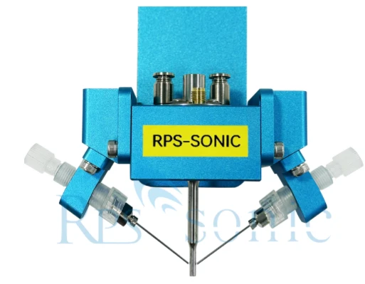
Ultrasonic photoresist coating equipment is a specialized device for photoresist coating based on ultrasonic atomization technology. It is primarily used in precision manufacturing fields such as semiconductors, panels, wafers, MEMS, and photovoltaics. It atomizes photoresist into nano/micron-sized ultrafine droplets, uniformly spraying them onto the surface of substrates such as wafers and glass substrates, replacing traditional spin-coating and dip-coating processes.
Simply put, it is the core equipment in the "resist coating stage" of the photolithography process, boasting advantages such as high precision, high uniformity, low resist consumption, and no swirling/thick edge defects, making it suitable for the photoresist coating requirements of advanced processes.
Core technological advantages (compared to traditional spin coating/dip coating)
Photoresist coating is a crucial pre-process step in photolithography, and the uniformity of film thickness directly affects the accuracy of photolithography. The core advantages of ultrasonic spraying equipment far surpass those of traditional processes, which is also the main reason for its widespread adoption in advanced manufacturing processes.
1. Ultra-high coating uniformity: Film thickness uniformity ≤ ±1%, eliminating the "thick edges and concave centers" of spin coating, suitable for the photolithography requirements of advanced processes such as 7nm/5nm;
2. Extremely low photoresist consumption: Spin coating has a photoresist consumption utilization rate of only 10~20%, while ultrasonic spraying can reach 80~95%, significantly reducing the cost of photoresist (a high-cost consumable);
3. Wide controllable film thickness range: Capable of coating thin films from 10nm to 100μm, suitable for both ultra-thin and thick photoresist layers (e.g., packaging photolithography, MEMS deep hole photolithography);
4. No mechanical stress damage: No centrifugal force or high-speed substrate rotation, avoiding wafer/substrate warping and cracking, suitable for fragile substrates (e.g., ultra-thin wafers, flexible substrates);
Adaptable to complex substrates: Adaptable to complex substrates: Can coat non-planar substrates, deep holes/ Grooved substrates, large-area substrates, and irregular shapes that cannot be processed by spin coating
Environmentally friendly and pollution-free: Low glue consumption, extremely low exhaust waste liquid volume, no glue mist splattering like in spin coating, meeting clean production requirements.